A new technique uses light to help print pure nanocrystals, opening the door to the photonic chips and super high-resolution virtual reality goggles.
In a breakthrough for the next generation of computer chips and virtual reality headsets, a team at Tsinghua used light as a catalyst to fuse nanocrystals into a series of intricate shapes. It’s hoped this technique will eliminate problematic polymer impurities associated with the 3D printing process. The study was published in Science in September 20221.

A Tsinghua University team have used their unique two-photon lithography-based 3D printing technique to create pure nanocrystal volumetric 3D structures.
Until now, the structural integrity of 3D printed nanocrystals demanded the use of polymer additives, explains Hong-Bo Sun, from the State Key Laboratory of Precision Measurement Technology and Instruments at Tsinghua University. But high functioning devices need to be 100% nanocrystal, he explains.
Postprocessing heat treatments used to remove the polymers, such as pyrolysis or calcination, can lead to severe structural shrinkage or defects: for instance, semiconductor nanocrystals often fuse and lose their luminescent properties. “Basically, a high percentage of polymer is good for structure formation, but it’s detrimental to functions, such as light emission,” says Sun.

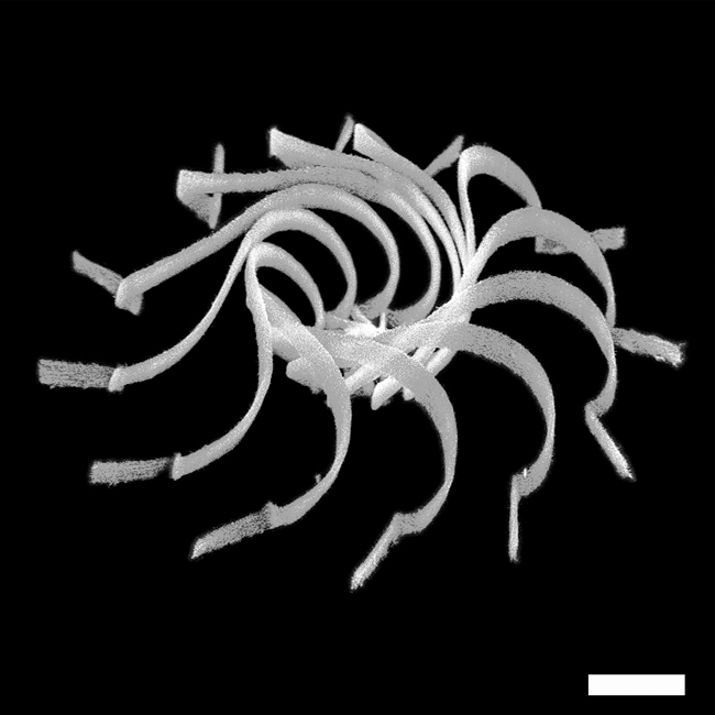
A Tsinghua University team have also used their new 3D printing technique to create curved structures from nanocrystals, without the addition of polymers.
Going towards the light
Polymers limit the integrity of 3D printed nanocrystals that could be used in very promising technologies—such as photonic integrated chips. These chips, which transmit data using photons of light instead of electrons, are being pushed as possible fixes to integration and heat generation problems in electronics, challenges slowing the development of smaller, faster and better devices.
Currently, active optoelectronic devices are usually built using a semiconductor epitaxial approach, a type of crystal growth or material deposition determined by a crystalline seed layer. But usable materials and device structures are quite limited, says Sun. More accessible photonic chips are thought to be key to the next big increase in capacity and data transmission speed.

Hong-Bo Sun works at the State Key Laboratory of Precision Measurement Technology and Instruments at Tsinghua University.
Clever clumping
Sun works closely with nano-optics and laser manufacturing expert, Linhan Lin, the other lead author on the 2022 paper. Their new 3D nanoprinting technique uses two-photon lithography—a process by which a beam of light from a laser induces the absorption of two photons into a material, triggering photochemical reactions that bond nanocrystal surfaces.
The idea for this method dates back to 1999, when Sun worked with another team that used two-photon induced photopolymerization to fabrication of a bull shape out of photocurable molecules. Their pioneering work was reported in Nature in 2001.
Polymers were, however, inherent in that process. “Since then, I have dreamed of building devices using pure nanoparticles without any adhesive,” says Sun. “Now we give a perfect solution to the problem using new quantum physics.”
To demonstrate the effectiveness of their idea, in 2022 the Tsinghua team used cadmium selenide/zinc sulfide core–shell quantum dots—the most popular semiconductor quantum dots. These, says Sun, have excellent light-emitting performance and stability, which will be useful in optoelectronic and photonic nanodevices. Excitation of their electron-hole pairs is also relatively easily induced by visible light in these materials.
Mimicking the photocatalysis process, the team then used light to excite the electron-hole pair and transfer the high-energy holes towards ligands that had been chemically linked to their nanocrystal’s surfaces forming a bridge. Using this technique, the group created everything from straight scaffold-like shapes to curly and 3D mechanical-seeming nanocrystal shapes.

Linhan Lin, a long-time collaborator with Hong-Bo Sun, also works at Tsinghua University’s State Key Laboratory of Precision Measurement Technology and Instruments.
Next-gen headsets
Pure nanocrystals could also be useful building blocks for microsensors or as part of devices for optical communication, sensing, and energy, says Sun.
And they could drive the development of cutting-edge virtual reality headsets, he adds. There is an ever-growing demand for a greater number of pixels in wearable near-eye displays for virtual and augmented reality devices. “Our technique printed high-resolution devices of less than 77 nm,” Sun points out. So in theory, he says, the technique could enable the printing of ultrahigh-resolution quantum dot light-emitting diodes (LEDs) with pixel resolutions of more than 100,000 dots per inch.
The next step is to see if the group can perform this process on a greater variety of nanocrystals, says Sun, and then to examine with industry the possibilities for new photonic/optoelectronic nanodevices.
Reference
Liu, S-F., Hou, Z-H., Lin, L., Li, F. & Zhao, Y. 3D nanoprinting of semiconductor quantum dots by photoexcitation-induced chemical bonding Science 377(6610), 1112-1116 (2022) doi: 10.1126/science.abo5345
Editor: Guo Lili