Machine learning technologies have been widely used in high-performance information-processing fields. At the same time, the requirements for computing capacity, speed, and energy consumption are increasingly high when solving complex tasks. However, the computing speed of existing hardware is severely limited by the traditional von Neumann architecture, and as the computing process takes longer, it becomes less efficient and consumes more energy. In recent years, optical and photonic computing methods have shown remarkable potential in performing deep learning processes involving complex calculations. Many institutions have successively proposed several architectures for integrated optical neural networks (ONNs), such as designs based on the Mach‒Zehnder interferometers (MZIs), micro-ring resonators (MRRs), and wavelength division systems etc. However, there is a problem of limited expansion of computing units in integrated ONNs at present, which severely limits the further improvement of computing capacity.

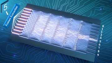
Fig. 1 Schematic diagram of integrated diffractive optical neural network
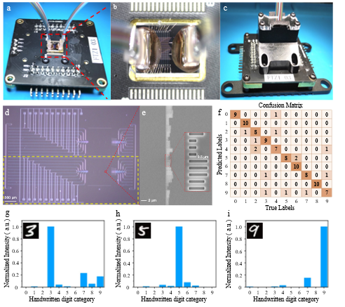
In this work, Professor Hongwei Chen’s group proposed an integrated diffractive optical neural network (DONN) based on subwavelength structures. The integrated DONN overcomes the volume limitation of spatial diffractive ONNs, which not only greatly improves the integration of computing units, but also reduces the errors caused by the large volume of optical elements and system calibration. For other integrated ONNs, the DONN gets rid of the restriction of the number of waveguides, which is easier to achieve large-scale expansion of computing units on the chip, thus solving the problem of high computing capacity of integrated ONNs. The computing throughput of the on-chip DONN implemented in this work can reach 1.38×10⁴ TOPS (TOPS: Trillions of operations per second), the computing capacity can reach 1016 FLOPS/mm2 (FLOPS: floating-point operations per second), and the energy consumption is about 10-17 J/FLOP (FLOP: floating-point operation). The integrated DONN chip’s fabrication is fully realized in China. The manufacturing process is compatible with the standard complementary metal oxide semiconductor (CMOS) process and meets the conditions for large-scale and low-cost production. Professor Hongwei Chen's group completed the theoretical exploration, simulation verification, structural design, layout drawing, chip processing, packaging, and system error compensation of the integrated DONN chip. This achievement may significantly improve the practicability of the integrated ONN chip and is expected to realize the integration of multiple DONNs on a single substrate so that the on-chip optical computing system will have larger processing capacity, which perhaps greatly promote the rapid development of integrated optical computing, photonic intelligence, etc.

Fig. 2 Physical picture of the DONN chip package, chip structure and experimental test results
This work was published in Nature Communications with the title of "Photonic machine learning with on-chip diffractive optics". The first author of this paper is Tingzhao Fu, a doctoral student in the Department of Electronic Engineering, and Professor Hongwei Chen is the corresponding author of this paper. Other authors include Professor Minghua Chen, and Associate Researcher Sigang Yang, etc. Department of Electronic Engineering, Tsinghua University.
This research was supported by the National Key Research and Development Program of China (2019YFB1803500) and the National Natural Science Foundation of China (NSFC) (62135009).
Fu, T. et al. Photonic machine learning with on-chip diffractive optics. Nature Communications 14, 70 (2023).
Full-text article: https://www.nature.com/articles/s41467-022-35772-7
Editor: Li Han

